Take 5 - The STM32F407

- An ARM 32-bit Cortex™-M4 CPU with FPU rated at 168MHz
- 192Kbytes of SRAM which includes 64-Kbyte of CCM (core coupled memory) data RAM
- A static memory controller supporting Compact Flash, SRAM, PSRAM, NOR and NAND memories
- General-purpose DMA: 16-stream DMA controller with FIFOs and burst support
- Loads of hardware timers
I bought a Discovery board which contained this chip. This board comes with nice 0.1" headers that I used to connect to my PAL encoder board (see previous posts) with short prototyping jumper wires.
Firstly I set-up a development environment. I use Linux and MacOS X at home and luckily this was really quite easy. I'm pretty productive on Eclipse so I set up fresh Eclipse Luna package and added:
- C/C++ Development Tooling (CDT)
- GNU ARM Eclipse Tooling
I'm running Ubuntu 14.04 so I also had to issue install cross-complier and debugger:
sudo apt-get install gcc-arm-none-eabi gdb-arm-none-eabiThe Discovery board has a neat ST-Link v2 interface on it which when sent certain commands over the USB connection will drive the SWD interface in the STM32F4 chip. This allows code on the STM32F4 chip to be debugged and also allows flashing of the chip. I used the following tool to talk ST-Link: https://github.com/texane/stlink
STLink provides a GDB-server interface which means that GDB (or Eclipse) can be used to debug code live on the device. Neato. So basically:
GDB/Eclipse -> GDB server (STLink) -> STLink v2 facade chip -> SWD target (STM32F4)It sounds like a lot of moving parts but it really isn't. This tool chain has work 100% of the time for me without a single issue. I have debugged on-chip at least 30 times.
It should be noted that Eclipse Luna has some bugs that stop the debugger from working. There is a bug report I can't recall but in a nutshell, the Step In/Over/Out controls remain disabled. It is a UI regression that doesn't exist in the previous Kepler release. Until fixed I suggest you use Eclipse Kepler.
The Architecture
Ok here comes the fun stuff: software. I chose to generate a PAL compatible sync signal right out of my STM32 chip. Other have generated a VGA (two signal sync) and fed that to the AD724 chip successfully. I wanted to stick with a PAL (single signal sync - say that fast) as illustrated in the diagram below: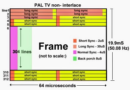
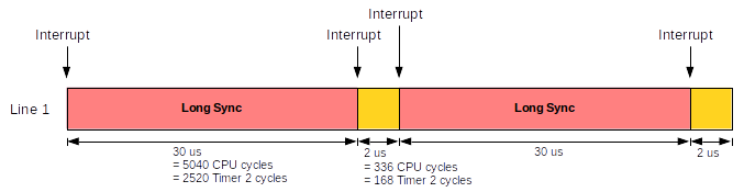
In my design I decided to interrupt on every transition above. So in the top-left corner above I'd interrupt at the end of the long sync at the transition to the small yellow region. At that point i'd set the next wake-up and go to sleep. This is illustrated below:
Timer 2 is used to generate this pattern. It runs at half the CPU clock frequency so in my case that was 84MHz. I'm using the Output Compare Channel 1 feature to generate the CPU interrupt every time a there is an Output Compare match. A lot of micro-controllers have Output Compare features and generally they are pretty simple. Usually you load a target counter value in a register and when the timer (or counter) reaches it, it takes some fixed of configurable action. The STM32F4 is no exception. I have it generate a CPU interrupt on match. When I wake up in the interrupt handler I just load the next counter value (plus the last value since I'm accumulating) and go back the sleep. If you are looking through the sources (when I get around to making them available) you'll see this code:
HAL_TIM_OC_Init(&frameTimer);
HAL_TIM_OC_ConfigChannel(&frameTimer, &frameOCConfigC1, TIM_CHANNEL_1);
HAL_TIM_OC_Start_IT(&frameTimer, TIM_CHANNEL_1);
These functions are found in the STM32 Cube SDK. STM32 Cube is a relatively new SDK from STM and therefore there isn't much example code around. You'll find most of the code out there either targets the Standard Peripheral Library (SPL) or registers directly. As far as I can tell the STM Cube SDK is the replacement for the SPL. Writing to registers directly was out of the question for me since I was going from Zero to Working in 4 weeks.
The vital parts of STM Cube are automatically dropped into your Eclipse project using the the wonderful GNU ARM Eclipse tooling described above. This really makes it easy to get going and yet you can still dig through the included source to find out what is going on under the hood. I had to do that a lot to get this to work. Unfortunelty the STM Cube SDK suffers from a lack of documentation and a lack of examples. I'm not saying that they don't exist, I just can't find them.
Generating the Sync pulse
So, how do I generate the Sync Pulse? The hardware does this for me with cycle-precision!
As well as generating an interrupt on OC match, I have configured this OC Channel to toggle it's associated GPIO pin on match. In this case the pin is PA0 which is buried in the manual. Firstly, I needed to switch GPIO Port A [0] to it's alternate function as follows:
GPIO_InitTypeDef GPIOA_InitStructure;
GPIOA_InitStructure.Pin = GPIO_PIN_0;
GPIOA_InitStructure.Mode = GPIO_MODE_AF_PP;
GPIOA_InitStructure.Speed = GPIO_SPEED_FAST;
GPIOA_InitStructure.Pull = GPIO_NOPULL;
GPIOA_InitStructure.Alternate = GPIO_AF1_TIM2;
HAL_GPIO_Init(GPIOA, &GPIOA_InitStructure);
This put the pin under control of the timer. So whenever there is an OC match I get a toggle on this pin for free.
Using hardware to control hardware
Using Timer 2 in the way described above great because the hardware is generating the time-critical events for me. I took this a step further for the pixel output stream. The diagram below shows the overall architecture of the system:

I'm using another Timer (Timer 1) to drive the DMA peripheral. Timer 1 is set to roll-over at 8MHz and is configured to generate a DMA Update event at that time. When the DMA peripheral received this update it transfers another byte it's configured source to destination. Timer 1 is set as a slave of Timer 2. I'm using another Output Compare channel (OC 2) to gate the Timer 1. When there is a match on OC 2, Timer 1 is allowed to tick. Latter on I force it off once I know the DMA transfer is complete so that next time it is ready to go again.
This kind of thing really appeals to my inner engineer. It is a great example of applying a set of constrained components to a problem and coming up with a solution within those constraints. In this case, the Timer and DMA peripherals are my building blocks and an have configured them to solves the problem with very little code required.
This gives me a jitter free pixel stream.
What next? Let's write a game!